SK Hynix's H-TPU: more than 100 tiny in-house processors split the SSD controller's workload
🕒 Published on Zendoric: October 15, 2026 · 00:13
✨ AI-generated · how it's made
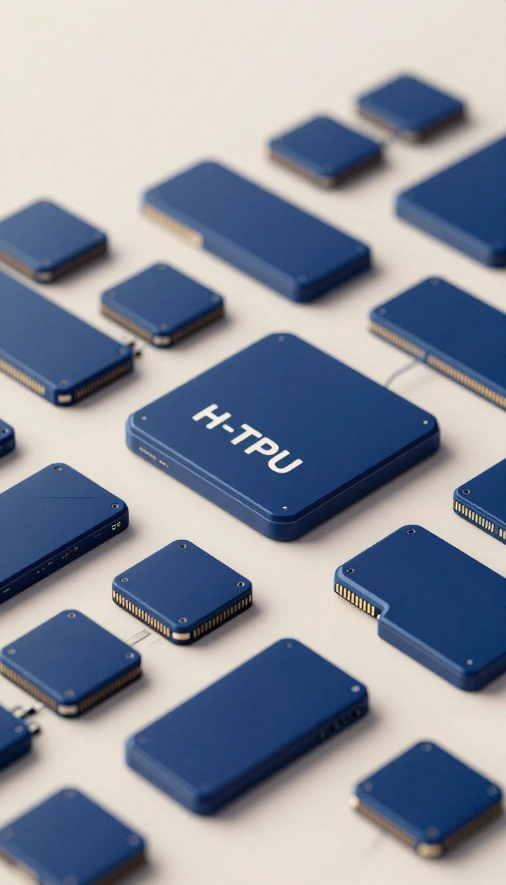
SK Hynix has unveiled the architecture and performance of its Hynix Transaction Processing Unit (H-TPU), a small in-house processor developed for solid-state drives (SSDs).
📚 Go deeper
The story of NVIDIA and Jensen Huang: how a video-game card company ended up making the most coveted resource on the planet.
As an Amazon Associate, Zendoric earns from qualifying purchases; the price does not change for you. · all our recommended books →
SK Hynix has unveiled the architecture and performance of its Hynix Transaction Processing Unit (H-TPU), a small processor developed in-house for solid-state drives (SSDs). According to The Elec, the technology spreads repetitive tasks that general-purpose CPUs have traditionally handled across more than 100 H-TPU units, with the aim of reducing power consumption and chip area.
The presentation was given by Koo In-je, vice president at SK Hynix, on October 12 at the International SoC Design Conference (ISOCC) 2026, held at Songdo Convensia in Incheon. Koo explained that the general-purpose CPUs inside today's SSD controllers are reaching their limits in power consumption and chip area, and that the H-TPU was designed to handle repetitive input/output (I/O) data transfer paths more efficiently.
The H-TPU is an ultra-lightweight programmable processor. It handles repetitive SSD operations such as processing read and write commands, managing metadata and controlling buffers. Until now, all of this was done by the controller's general-purpose CPUs. As SSD performance has increased, the workload has demanded more CPU cores, which has inflated both processor area and power consumption excessively.
According to Koo, the Arm CPU cores commonly used in SSD controllers are oversized for simple, repetitive tasks. They are optimized for complex, high-speed computation, so using them for simple operations wastes power and area. In addition, their architecture is not well suited to splitting work into small tasks and distributing them across multiple processors.
The H-TPU features a four-stage pipeline and an in-order execution structure suited to repetitive workloads. Unlike a monolithic CPU, multiple H-TPUs can be distributed across the controller and assigned to specialized functions. The main general-purpose CPU is reserved for complex tasks such as error recovery, exception handling and storage policy management.
SK Hynix has integrated more than 100 H-TPUs into its SSD controller architecture. When an I/O request arrives, only the H-TPUs dedicated to the required functions are activated, while the rest remain idle to save power. According to the company, a single H-TPU consumes roughly 2.5% (one-fortieth) of the power and occupies about 4% (one twenty-fifth) of the chip area of a standard general-purpose CPU core.
Koo summarized the approach as follows: SK Hynix broke down the read and write processes of traditional SSD controllers into smaller tasks and structured the system so that numerous H-TPUs process them in parallel. The company has also developed software tools, including a dedicated compiler, so that engineers can write specialized code more effectively.
As for deployment, SK Hynix plans to apply H-TPU technology to several NAND flash product lines, starting with next-generation enterprise SSD (eSSD) controllers. It will later be integrated into Storage Next, the company's next-generation storage architecture for AI, and into high-bandwidth flash (HBF), slated for launch next year. Storage Next is optimized for the fine-grained data access required by modern AI models and handles units as small as 512 bytes, one-eighth the size of conventional 4-kilobyte units.
Note: the power and area figures come from SK Hynix itself and the original article; the text provides no absolute performance data (IOPS, latency) or specific production dates for H-TPU-based products.
📚 Go deeper
The reference manual for building products on top of AI models: prompts, RAG, fine-tuning, agents, evaluation and deployment.

Semiconductors as the oil of the 21st century: history, espionage, and why an island of 23 million people underpins the entire AI economy.
As an Amazon Associate, Zendoric earns from qualifying purchases; the price does not change for you. · all our recommended books →
🔗 Related on Zendoric
- OpenAI's first hardware isn't a phone: it's a controller for giving orders to coding agents · 2026-07-16
- Microsoft launches in-house AI models it says cut costs by up to 89% versus OpenAI · 2026-07-28
- The AI safety split is now state business: Huang pressed Amodei at the White House minutes after both signed · 2026-10-05