The Economist: chip manufacturing turns vertical as Silicon Valley-style miniaturization runs out
🕒 Published on Zendoric: July 10, 2026 · 00:24
Important note: the content downloaded from this link to The Economist is only the teaser preceding the paywall. Only the title, the standfirst and the first introductory paragraph of the article could be retrieved; the rest —the technical development, concrete company examples, figures or…
📚 Go deeper
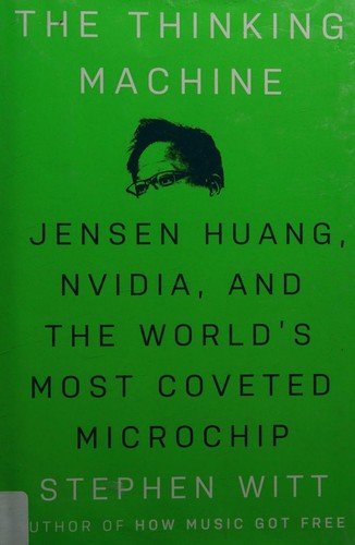
The story of NVIDIA and Jensen Huang: how a video-game card company ended up making the most coveted resource on the planet.
As an Amazon Associate, Zendoric earns from qualifying purchases; the price does not change for you. · all our recommended books →
We'll send you a confirmation email (double opt-in). Privacy.
Important notice: the content downloaded from this The Economist link is only the teaser preceding the paywall. Only the headline, the standfirst and the first introductory paragraph of the article could be retrieved; the rest —the technical development, the concrete company examples, figures or statements— is not available in the received text. Therefore, this summary is deliberately brief and sticks strictly to what appears literally in that fragment, without filling gaps with assumptions.
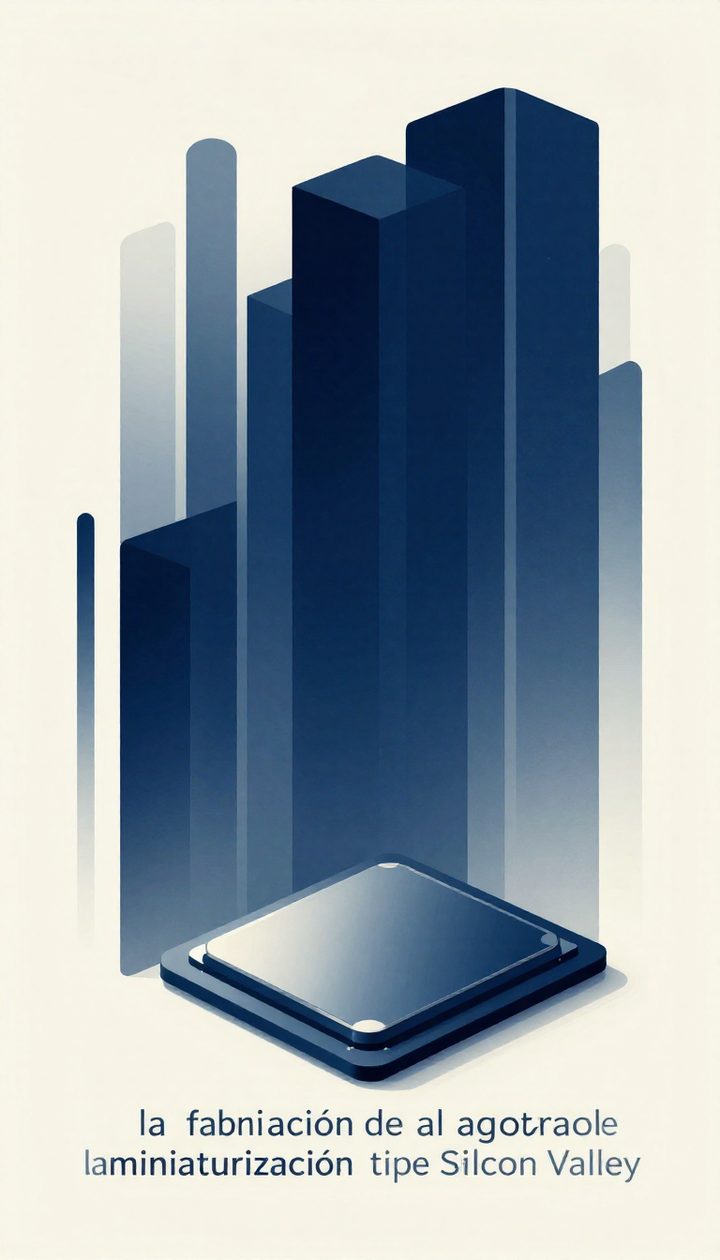
What the teaser does say: the article, published on July 8, 2026 in The Economist's Science and Technology section (print edition of July 11, 2026, under the headline "Manhattan on my mind"), poses an urban-planning metaphor to describe a paradigm shift in the semiconductor industry. Silicon Valley, the text says, is a low-rise region —offices, bungalows and shopping malls—, and the chips that give it its name have traditionally been manufactured in an analogous way: millions of transistors (the electrical switches that encode the binary ones and zeros, the basis of computing) are placed side by side on a silicon wafer, on an essentially horizontal plane.
The article states that, over the past half-century, the industry has pursued more performance by shrinking transistors and packing them ever more densely on that horizontal plane —the logic underlying Moore's Law. But, according to the text, that resource is running out of road. The consequence, presented as the article's central thesis, is that chipmakers are finally starting to build upward: stacking in height rather than only spreading out across the surface. Hence the metaphor that gives the piece its title: the future of chip manufacturing will look less like California's horizontal sprawl and more like Manhattan's vertical skyscraper profile.
The retrieved fragment does not include technical details on how this vertical construction is achieved (for example, which 3D stacking techniques, which companies are implementing them, timelines, costs or performance figures), nor does it explicitly mention political or geopolitical factors beyond the section label ("Constrained by physics and politics") that appears in the subtitle. Nor is it possible to confirm additional content that would normally follow in the body of the article, since the rest of the downloaded text corresponds to website navigation, links to other articles and legal/cookie notices, unrelated to the topic.
In short: the central idea —supported only by this fragment— is that the horizontal miniaturization of transistors, the traditional engine of Moore's Law, is approaching physical limits, and that the industry's response involves the vertical stacking of components ("3D acceleration," according to the article's editorial label). For a full analysis of which specific technologies, players and timelines are cited, it would be necessary to access the full article, currently behind The Economist's paywall.
📚 Go deeper

Semiconductors as the oil of the 21st century: history, espionage, and why an island of 23 million people underpins the entire AI economy.

Algorithms in justice, medicine, cars and art, explained with British humor and mathematical honesty.
As an Amazon Associate, Zendoric earns from qualifying purchases; the price does not change for you. · all our recommended books →
🔗 Related on Zendoric
Sources & references
Get the analysis by email · free
One email a day analysing the AI essentials. Free, no spam, unsubscribe anytime.
We'll send you a confirmation email (double opt-in). Privacy.